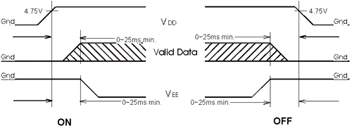
Figure 7.1: Power Supply Sequence
To prevent latch-up of the CMOS LSI (HD61830(B) and LCD driver LSI) ensure your systems power supply follows the following sequence. The VDD must be applied with a small time delay befor VEE is turned on. It is very important to follow this sequence in order to prevent the CMOS LSI from latching up and to prevent DC signals from being applied to the LC material. If the VEE voltage is applied before the timing signals M, CL1, CL2, and FLM then a DC voltage will be applied to the LC material. Over time this will degrade the LC fluid performance due to their electro-chemical behavior. If this power-up sequence is not adhered to, permanent damage to the LCD module may result.
Figure 7.1: Power Supply Sequence
The RESET circuit shown in Figure 7.2 is recommended to correctly reset the HD61830(B). On RESET the internal registers of the HD61830(B) are cleared and the BUSY flag is reset, Display is turned off, HP=6 and HD61830 is set for Slave mode (Refer to section 8 for detail).
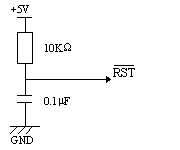
Figure 7.2: RESET Circuit
Next Section