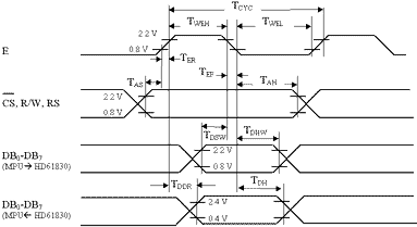
Figure 5.1: MPU Interface Timing (MPU - HD61830(B))
| Item | Symbol | Min | Typ | Max | Unit | |
|---|---|---|---|---|---|---|
| Enable cycle time | tCYC | 1.0 | - | - | Ás | |
| Enable pulse width | "H" | tWEH | 0.45 | - | - | Ás |
| "L" | tWEL | 0.45 | - | - | Ás | |
| Enable rise time | tEr | - | - | 25 | ns | |
| Enable fall time | tEf | - | - | 25 | ns | |
| Set up time | tAS | 140 | - | - | ns | |
| Data set up time | tDSW | 225 | - | - | ns | |
| Data delay time | tDDR | - | - | 225 | ns | |
| Data hold time (Write) | tDHW | 10 | - | - | ns | |
| Address hold time | tAH | 10 | - | - | ns | |
| Data Hold Time (Read) | tDH | 20 | - | - | ns | |
| Pulse width of /RES | tWRES | 1Ás | - | 2ms | - | |
Note: MPU interface timing for HD61830B is identical to HD61830
Figure 5.1: MPU Interface Timing (MPU - HD61830(B))
| Item | Symbol | Min | Typ | Max | Unit | |
|---|---|---|---|---|---|---|
| Clock pulse width (high level) | tWCL1 | 450 | - | - | ns | |
| Clock delay time | tDCL2 | - | - | 200 | ns | |
| Clock cycle time | tWCL2 | 900 | - | - | ns | |
| Clock pulse width | "H" | tWCH | 450 | - | - | ns |
| "L" | tWCL | 450 | - | - | ns | |
| M delay time | tMD | - | - | 300 | ns | |
| FLM delay time | tDF | - | - | 300 | ns | |
| Data delay time | tDD | - | - | 200 | ns | |
| Data set up time | tSD | 250 | - | - | ns | |
Note: No load is applied to all outputs.
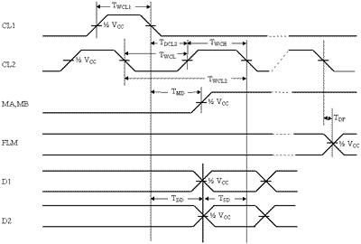
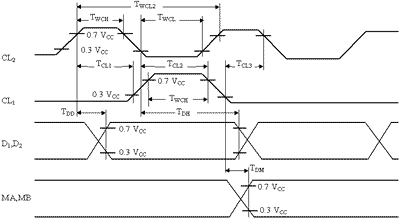
Figure 5.2: LCD Interface Timing (HD61830 - LCD)
| Item | Symbol | Min | Typ | Max | Unit | Note | |
|---|---|---|---|---|---|---|---|
| Clock cycle time | tWCL2 | 416 | - | - | ns | 1 | |
| Clock pulse width | "H" | tWCH | 150 | - | - | ns | 1 |
| "L" | tWCL | 150 | - | - | ns | 1 | |
| Data delay time | tDD | - | - | 50 | ns | 1 | |
| Data hold time | tDH | 100 | - | - | ns | 1 | |
| M delay time | tDM | -200 | - | 200 | ns | 1 | |
| FLM set up time | tSF | 400 | - | - | ns | 2 | |
| FLM hold time | tHF | 1000 | - | - | ns | 2 | |
| M set up time | tSMA | 400 | - | - | ns | 2 | |
| M hold time | tHMA | 1000 | - | - | ns | 2 | |
Note 1 -
Note 2 -
Figure 5.3: LCD Interface Timing (HD61830B - LCD)
Next Section