 |
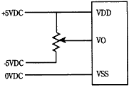 |
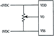
| +5VDC Input LCD Module | +/-5VDC Input LCD Module |
Modules require +5V at 1 to 10 milliamps. Extended temperature and some high contrast modules require -5V, also at low current. Inexpensive ICs convert +5V to -5V efficiently. If the display has backlighting, required power must also be budgeted. The power supply does not have to "lock-on" +5V but it must not "spike" beyond the module's absolute maximums.
A module's logic circuits have 3 connections to the power supply: VDD (+5VDC); VSS (Ground); and VO, viewing angle adustment, sometimes called contrast or bias control. The diagrams below show typical connections. Contrast can also be controlled digitally with a digital potentiometer or DAC.
|
|
| +5VDC Input LCD Module | +/-5VDC Input LCD Module |
Power Supply to Module Connection
LCD modules have a limited operating temperature range. (See exact model for specific limits). The fluid within the glass is the most limiting factor. Over the rated range, the bias, or VO voltage required to optimise the contrast and maintain a constant viewing cone varies slightly. Compensation or adjustment can be achieved manually, with a tem-erature compensation circuit, or a combination of both.
Manual adjustment involves user accessible control via a potentiometer or digital device as explained above. A standard, negative temperature coefficient thermostat serves as an inexpensive, automatic sensor. It should be mounted as close to the glass as possible to get an accurate measurement. A thermistor circuit can be configured to provide automatic temperature compensations. Each module's specification lists approximate VO voltages required at the extremes of the temperature range and at 25C. A suggested circuit is shown below.
When operating outside of the module's rated temperature range, forced
air and/or a heater are required to maintain reliable operation. The heater manufacturer
can offer design assistance. 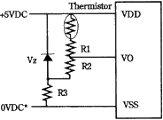
LCD Module
*For displays requiring -5VDC, R3 should be connected to -5, VSS to
ground.
Temperature Compensation Circuit Example
Notes:
1) Typical termistor value 15k @ 25C, B=4300
2) R1 and R2 values are selected based on required VO level. See module specifications.
3) R1 and R2 can be variable resistor for manual control.
4) Vz value = 4.5V for1/8 & 1/11 duty cycle displays: 5.0V for 1/16 duty cycle; 10V
for modules using +/-5V supply.
A/N modules are an intelligent peripheral which can communicate, bi-directionally, within the master system. Tie the device into the system data bus and treat it as RAM, I/O, or expanded, parallel I/O. The module is "selected" by gating a decoded, "module-address" output, with the host processor's "read or write" strobe. The resultant signal, applied to the LCDs "enable" input, clocks in data. There is no conventional "chip-select".
Interfacing the module to an existing micro-system involves:
a) joining the module to the host's data bus.
b) developing a "strobe" signal for the "E" signal
c) applying appropriate signals to modules "RS" and "R/W"
d) applying the proper "viewing angle" voltage to the display's VO pin.
Suggested interface circuits for most popular microprocessors are whoe on pages 16 and 17.
LCD modules provide a complete display subsystem which must be properly interfaced to the host micro-computer. The modules are classified as a "slow" periphera. Both access and strobe times exceed those normally encountered. A successful marriage requires strict attention in detail.
The Enable ("E") signal is the key signal line. This signal "clocks" the data and control signals into the LCD's internal microcontroller. The "E" signal must be a clean, positive going, digital strobe, which is active while data and control information are stable and true. The modules do not have a chip select line and so a decoded, host "select" signal must be geared with a proper strobe to generate this "E" signal. All module timing is referenced to specific edges of the "E" signal. The "E" signal is applied only when a specific module transaction is desired.
The "E" strobe must be 450 nS wide, minimum. It has a minimum period of 1000nS. The "E" line would only be pulsed this often during a "read" of the busy flag, performed during a "polled" display routine. Normally "E" strobes would be approximately 40 microseconds apart - which is the maximum display throughput. (See Instruction Table for complete list of execution times).
The 2 control lines, RS and R/W, must set-up 140 nS prior to the activation, or rise, of "E". These signals must remain stable, and hold for 10nS at the fall of "E". When a parallel port supplies RS, R/W and "E", do not allow these lines to all change together. This would result if a single instruction was employed and would surely violate the set-up requirement. Instead a second instruction must independently set the "E" bit high, after RS and R/W have been set. When the "E" signal is derived from a host strobe signal, it is only necessary to choose address or control signals which meet the 140nS demand. A single instruction transfer would be perfectly valid in this case - and is the goal.
When the host outputs RD and WR strobes these should not be linked to the module's R/W line. Since this same signal provides the "E" signal a set-up violation will occur. In this case it is preferable to use an address bit which sets-up earlier in the host's machine cycle. This is a crucial point.
The data bus must set-up 195 nS prior to the fall of "E". Atain these lines must hold for at least 10nS after "E" falls. Most host strobes should meet these requirements without difficulty.
The classic problem is encountered when the host micro is running so fast that the strobes are too narrow (450nS) to serve as the "E" pulse. In this case: a) prolong thewe pulses by using the host's "ready" input, b) prolong by employing that mode which extends timing, or c) decrease the host's crystal frequency. When these options are not viable it will be necessary to latch both the data and control information and then activate the "E" signal.
Timing diagrams and suggested interfaces to various common microprocessors are in the appendix.
Care must be taken when mounting an LCD module to ensure that module is not stressed when installed and the surface is not exposed to scratches or harmful material.
Causing any kind of warp on the PCB of the module may product open columns or rows of dots, or intermittent display. Presure on the bezel from the top or against the bezel tabs will lead to similar problems.
The front surface of the module is a sensitive plastic polarizer, not glass. Liquid must not be allowed to condense upon the device. Whenever possible, install an optically correct "protection Barrier" between the outside world and the display. This should be a non-polarized plastic or polycarbonate, which will reduce the incidence of foreign-object invasion and static discharge into the display. To keep glare at a minimum, mount the protective piece as close to the display surface as possible while preventing pressure on the piece from being transmitted to the LCD. Non-glare properties can be added to the protective piece at a slight loss of display clarity.
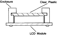
Mounting Suggestion